According to researchers at Peking University, Tsinghua, and HKU, the new method can slash lithography defects by a 99 per cent.
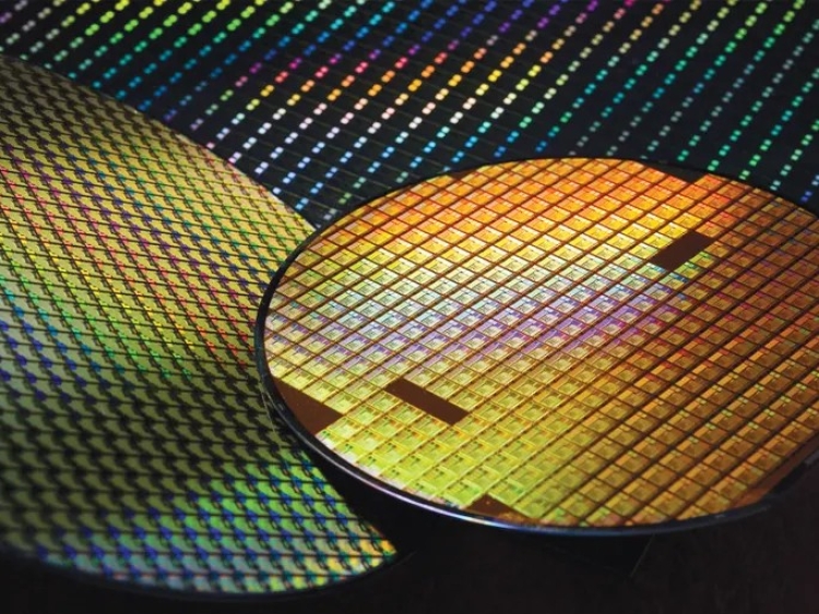
One of the trickiest bits of making semiconductors is photolithography, where light is used to “print” circuits onto silicon wafers. It’s rather like developing a microscopic photograph, except it costs billions and breaks more often.
The process involves spreading a photoresist, a light-sensitive goo, over the wafer. Ultraviolet light then shines through a mask that carries the circuit pattern, and the exposed material is chemically developed so some bits dissolve while others stay put. What remains forms the stencil for the later steps, like etching the metal or silicon layers.
That’s all well and good until the photoresist starts misbehaving. During development, dissolved material sometimes clumps together into microscopic particles that can stick back onto the wafer. At five-nanometre or smaller nodes, even a 30-nanometre blob can ruin a circuit.
Professor Peng Hailin’s team decided to use cryo-electron tomography (cryo-ET), a technique borrowed from biologists who use it to peek inside cells. They froze the developer solution to –175°C mid-reaction, capturing the photoresist’s behaviour in 3D using electron tomography. For the first time, chipmakers could actually see what was going wrong instead of guessing.
What they found was a microscopic mess. The photoresist polymers tangled up like spaghetti through weak hydrophobic interactions, forming 30–40 nm clumps. Around 70 per cent of the molecules didn’t even dissolve properly, instead floating at the air-liquid boundary until they were redeposited during rinsing.
Armed with this grim view of chip chemistry, the team made two quick fixes that play nicely with existing fabs. They raised the post-exposure bake temperature slightly, reducing polymer tangling, and reworked the rinse step so that the developer flow carried the clumps away before they could reattach.
When they tried it on 12-inch wafers, defect counts fell by more than 99 per cent, bringing near-perfect lithography quality within reach.