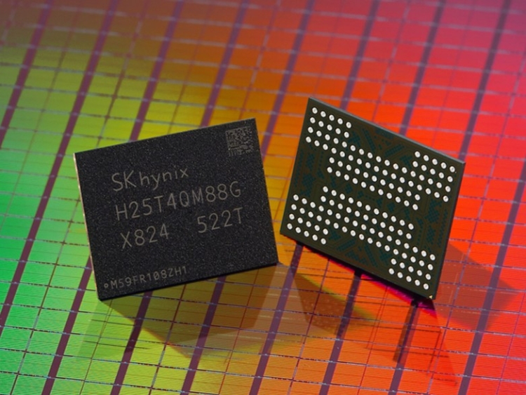
The Korean memory maker slid the gear into its M16 plant in Icheon, claiming the move will let it pump out next-generation DRAM with more density and better cost competitiveness. The firm boasted in a blog post that this cements its place as the go-to shop for customers like Nvidia and AMD.
ASML’s TWINSCAN EXE:5200B, the first of the High-NA production line, can print transistors 1.7 times smaller than current EUV gear, with density 2.9 times higher. The numerical aperture bumps from 0.33 to 0.55, which is a big leap in lithography terms.
In its announcement SK Hynix said: “With the introduction of High-NA EUV, we will be able to further simplify our process technology while accelerating the development of next-generation memory products to provide greater performance and competitiveness.”
Samsung is playing catch-up. It is not expected to get its first High-NA tool until later this year, with commercial deployment pencilled in for the end of 2025. TSMC, which normally sets the pace in bleeding-edge silicon, has also been beaten to the punch.
By getting there first, SK Hynix has managed to turn itself from Samsung’s underdog rival into a memory powerhouse in its own right, and it shows no sign of easing off the accelerator.